PCBs are the beating heart of modern electronics. From your phone and your car to medical devices and defense systems, if it runs on electricity, it probably runs on a PCB.
The global printed circuit board market is projected to reach nearly $68.5 billion by 2025 with a 6.7% compound annual growth rate. That’s impressive growth, especially after the supply chain setbacks caused by COVID-19. So, how are these essential pieces of tech actually made?
Let’s walk through it.
What Are Printed Circuit Boards?
A Printed Circuit Board (PCB) is a board that connects and supports electronic components. But unlike older tech, PCBs do this without using traditional wires.
Instead, they rely on an organized system of pads, traces, capacitors, resistors, and more to move and regulate electrical current. It’s a clean, compact, and efficient way to bring electronics to life.
Before PCBs, electronics relied on point-to-point wiring. It worked, but it was bulky, unreliable, and prone to failure as insulation aged. The rise of cheaper, smaller electronics led directly to the widespread use of printed circuit boards.
Common PCB Components
- Batteries – supply voltage to the circuit
- Resistors – regulate electrical current
- Capacitors – store electrical charge
- Connectors – link devices together
- Diodes – allow current to travel in only one direction
- LEDs – diodes that emit light
- Relays / Switches – control circuit flow
- Transistors – amplify electric signals
- Inductors – oppose sudden changes in current
PCB Terminology to Know
- Pads – exposed metal areas where components are soldered
- Paste Stencil – thin sheet that applies solder paste in exact spots
- Surface Mount – components soldered directly onto the surface (today’s standard)
- Through Hole – components with leads passed through drilled holes
- Traces – copper paths that carry current
- Solder – metal used to bond components and conduct electricity
Layers of a PCB
PCBs are made up of layers, each with a unique purpose. Together, they create a durable, functional platform for electronics.
- Layer 1: Base Material – usually fiberglass, gives the board structure
- Layer 2: Copper – laminated foil forms the conductive pathways
- Layer 3: Solder Mask – protective green coating that insulates copper
- Silkscreen – text and symbols printed for easier identification
Single-sided boards have one copper layer. Double-sided boards have two. Multi-layer boards can include many layers for more complex devices.
How PCBs Are Made
Here’s a high-level breakdown of the process:
- Create the fiberglass base
- Laminate copper layers
- Etch away excess copper to leave traces
- Apply the solder mask for insulation
- Add silkscreen for labeling
- You now have a blank board — time to populate it
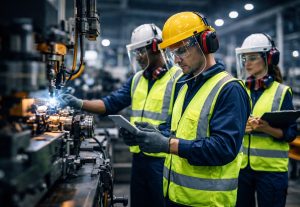
How PCB Components Are Added
There are two main ways to populate a PCB:
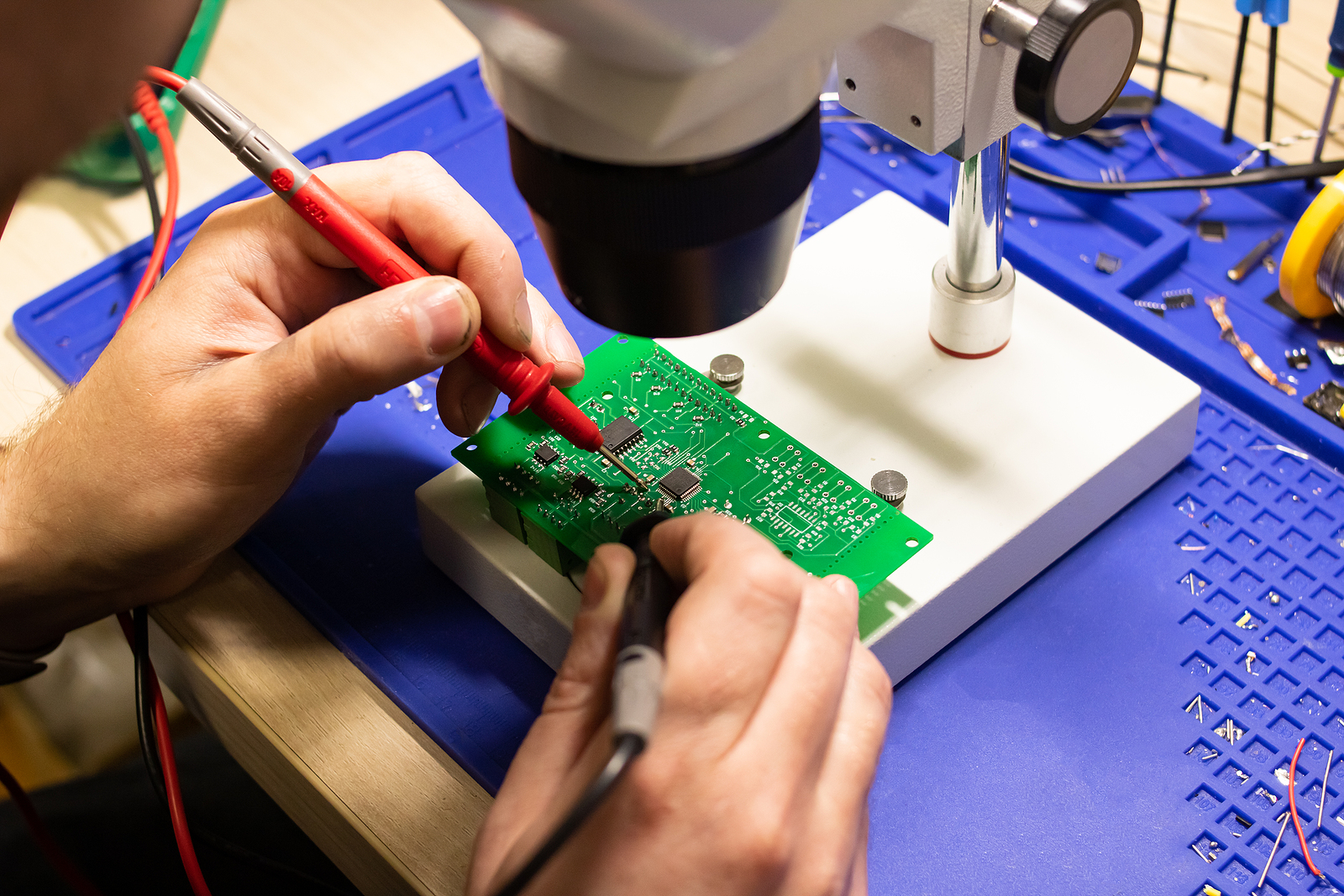
Hand Soldering
- Technicians work from labeled prints and kits
- Each component is placed and soldered by hand
- Great for prototypes and small production runs
- Here’s a look at hand soldering in action
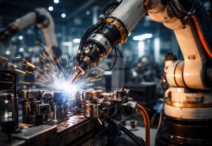
SMT (Surface Mount Technology) Machine Operations
- Boards move along a conveyor through multiple machines
- Components are placed, soldered, inspected, and packaged
- Ideal for large-scale production of less complex boards
- See SMT machines at work here
Examples of PCBs
Blank Board – a clean, component-free circuit board, ready for population
Populated Board – a finished PCB with components mounted and soldered
For a visual of the full PCB manufacturing process, the team at FlexTrades recommends this industry resource and encourages you to dig deeper.