In this edition of How It’s Made, we’ll be talking Printed Circuit Boards (PCBs). It’s a pretty hot topic right now. The printed circuit board market is set to reach nearly $68.5 billion worldwide by 2025. At the same time, this industry is set to have a compound annual growth rate (CAGR) of 6.7%. Which is fantastic news considering the most recent complications that COVID-19 added to PCB manufacturing and supply chain. With that news, we thought we’d give you some extra insight into just how PCBs are manufactured.
PCBs / Printed Circuit Boards – What Are They?
PCBs are boards that electronically connect electronic components through mechanical support. What does that mean, though? PCBs support electronics and electronic components but do so without wires! How is that possible, you ask? PCB components include pads, tracks, capacitors, and resistors, and more. More on that later, though!
Prior to PCBs, there were point-to-point wired boards. Although these did the job, they would often short-circuit when wire insulation began to age or crack and when wire junctions caused failures. Additionally, electronics became more prevalent in consumer goods over time (as well as cheaper and smaller), leading to the PCB.
PCB Components & Terminology
PCB Components
- Batteries: provide the voltage to the circuit.
- Resistors: control electrical current/flow through a circuit.
- Capacitors: store electrical charge.
- Connectors: provide connections of devices to another device.
- Diode: provide direction for the current. Current can only travel in one direction.
- LEDs: diodes that emit light. Lights up when current flows through it.
- Relays/Switches: operate electrically opening/closing circuits, as needed, for current flow.
- Transistors: amplify charges.
- Inductors: work to oppose any sudden changes in the current.
PCB Terminology
- The exposed metal on the surface of the board, where components are soldered are called pads
- The thin stencil that lies over the board, allowing solder paste to be deposited in specific areas during assembly is called paste stencil
- A way to build boards without requiring the component to have leads for soldering purposes (which are passed through hole boards) is called Surface Mount. This is the dominant type of board used today.
- Another way to build boards includes Through Hole. In this way, boards require components to have leads, which are pushed through holes on the board before soldering.
- The continuous path of copper on a circuit board is called trace.
- The metal that makes the electrical connections between the surface of the board and the electronic components also acts as a strong adhesive for the components. This is called Solder.
PCB Layers
- PCBs consist of multiple layers of heated and laminated material. Then, the multiple (and various) types of components mentioned above are soldered on to the board (in very specific ways) to allow the electrical charge to flow and guide it to the correct destination.
Board Layers
PCBs consist of multiple layers, with each layer performing a basic function pertinent to the placement of components and for the intended end use.
Layer 1: Base Material
- Typically, fiberglass. This provides the strength/rigidity of the board and varies in thickness according to end use.
Layer 2: Copper
- Heat and adhesive laminates a thin copper foil (and copper patterns) to the board. Lamination can occur on one side (single layer boards) or on wo sides (double layer boards). Multi-layer boards will have multiple sets of base material/copper layers.
Layer 3: Solder Mask
- Next, Solder Mask covers the copper while keeping pads and rings exposed. This is the green part of the board. This insulates the copper and protects it from contact with solder, conductive bits, or other metal.
Silkscreen
- This is the layering on top of soldermask. This adds the letters, numbers, and symbols to the board for easy assembly as well as understanding of the board. Typically, white but can be any color.
The Making of PCBs
The general process for manufacturing PCBs is:
- Creating the fiberglass core board.
- Laminating copper layers and pattern on top of fiberglass core board.
- Bathing the board to remove unwanted copper, leaving only the traces.
- Applying soldermask as a protective layer.
- Applying silkscreen which provides the pattern for component placement.
- We now have a bare/blank board.
- Adding PCB components.
There are two ways to add PCB components. Hand soldering or SMT machines. I explain both below.
Hand Soldering
- Boards are blank (or bare) with an outline printed of what types of components go where, to include numbered/labeled components.
- Solder Technicians hand solder a kit of components to the bare/blank board.
- Technicians work from print, work instructions, and kitted materials.
- You can find an example of hand soldering here.
SMT Machine Operations
- SMT (Surface Mount Technology)
- A series of machines operate in a line to manufacture Printed Circuit Boards by pushing bare/blank boards down the line on trays or conveyors. Each build operation (loading, placement, coating, printing, curing, inspection) occurs in a proper sequence. SMT lines increase the speed and quantity of PCB production and are also ideal for less complex boards. You can find an example of this Machines in this process include do a variety of tasks including placing components on the board, coating/sealing, soldering components, screen printing, melting solder, inspecting, and stacking.
- You can find an example of SMT Machines here.
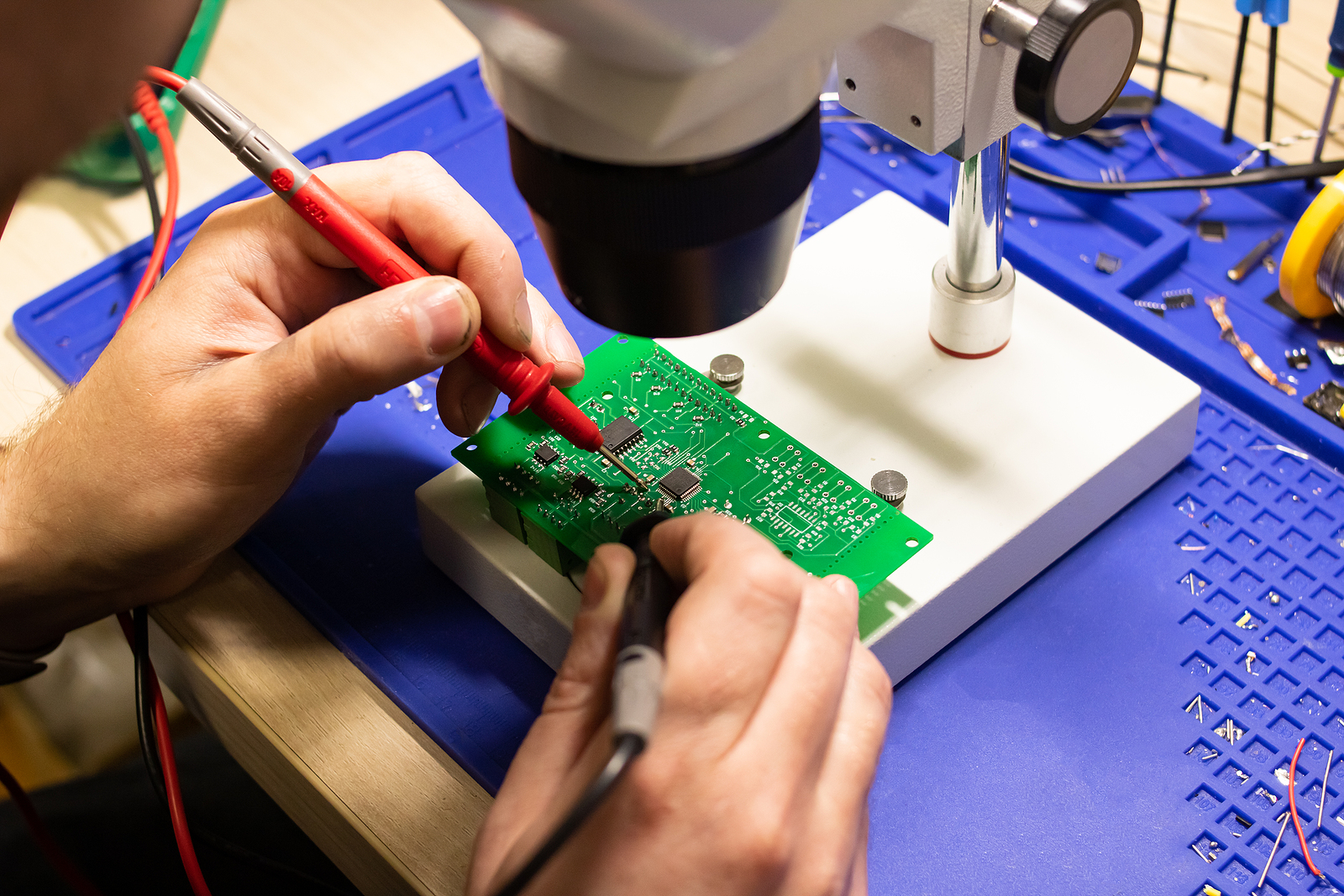
Below are two examples of PCBs – blank/bare board and a populated board.
Blank Board
Populated Board